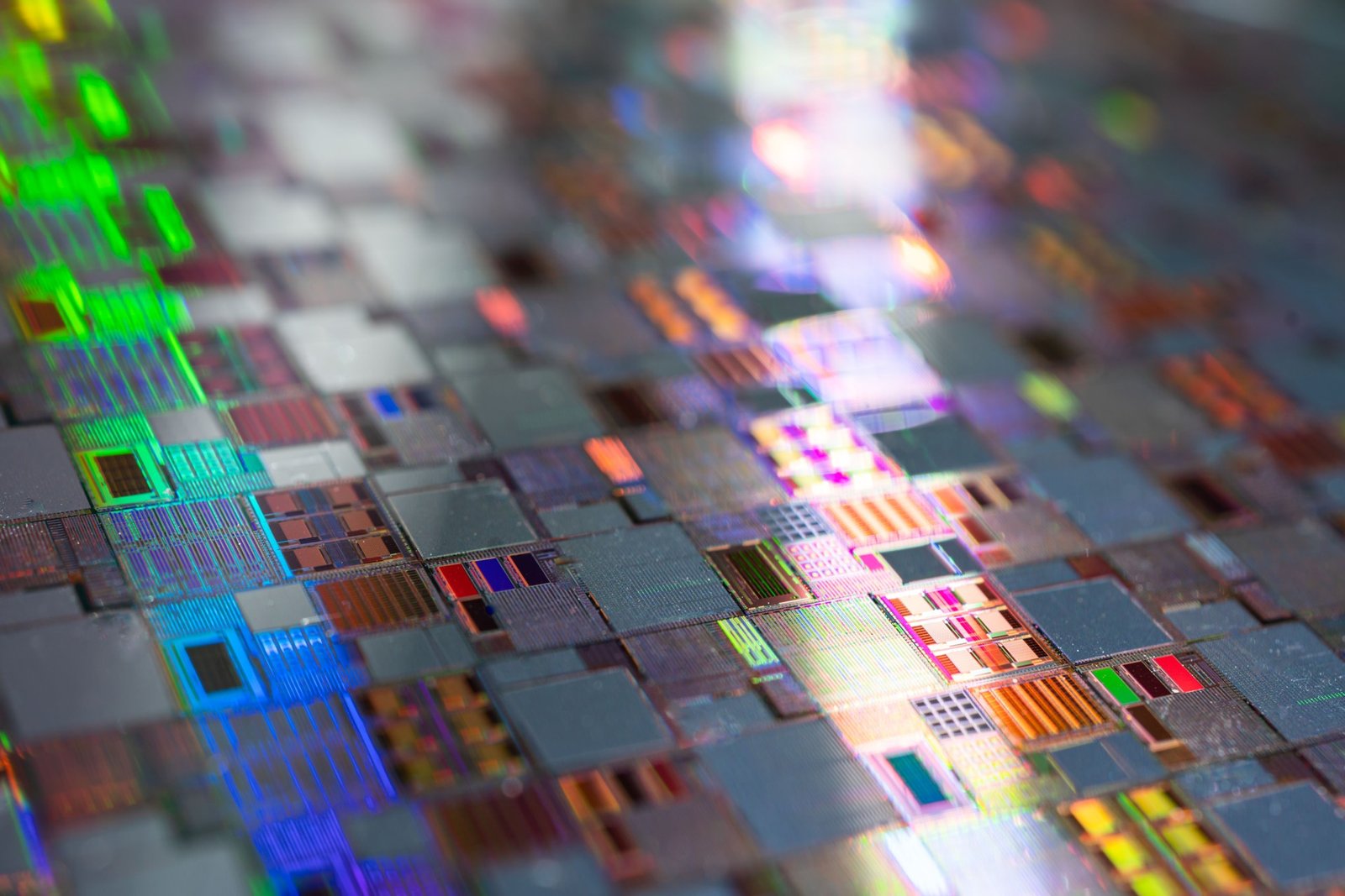
A silicon wafer is a thin, flat slice of crystalline silicon that serves as the foundation for fabricating integrated circuits (ICs) and various semiconductor devices. Silicon wafers are essential components in the electronics industry, forming the basis for microchips, computer processors, memory devices, and even solar cells. Silicon, a semiconductor material, is ideal for this purpose due to its excellent electrical properties, abundance, and ease of processing.
In this article, we’ll explore what silicon wafers are, how they are made, and their crucial role in the development of modern technology.
What is a Silicon Wafer?
A silicon wafer is a highly purified, flat disc made from silicon that has been crystallized and sliced into thin sheets. These wafers serve as substrates, or base materials, on which microelectronic components like transistors, capacitors, and resistors are fabricated. The circuits etched into the wafer during manufacturing form the heart of modern electronic devices.
Silicon wafers vary in diameter, ranging from 100 mm (4 inches) to 300 mm (12 inches) or more, with smaller wafers often used for specialized applications and larger wafers for mass production of semiconductors.
Key Properties of Silicon Wafers
Silicon wafers have several properties that make them ideal for use in semiconductor devices:
- Semiconductor Nature: Silicon is a semiconductor, meaning it can conduct electricity under certain conditions but act as an insulator under others. This ability to control electrical conductivity makes it perfect for creating electronic components like transistors and diodes.
- Crystalline Structure: Wafers are made from single-crystal silicon, which ensures that the atoms are perfectly aligned in a consistent pattern. This uniformity is critical for ensuring the proper functioning of semiconductor devices.
- Flatness and Smoothness: Silicon wafers are polished to extreme flatness and smoothness, with surface irregularities measured in nanometers. This level of precision is essential for microelectronics fabrication, where even tiny imperfections could disrupt the operation of devices.
- Dopability: Silicon wafers can be doped with impurities like boron or phosphorus to modify their electrical properties. This process creates regions with different electrical characteristics, which are necessary for constructing integrated circuits.
How Are Silicon Wafers Made?
The process of making silicon wafers involves several steps, each of which is critical to achieving the necessary purity and crystalline structure for semiconductor manufacturing. Below is a simplified version of the silicon wafer manufacturing process:
- 1. Purifying Silicon: Silicon is extracted from silica (SiO₂), commonly found in sand and quartz. The raw silicon undergoes a purification process, where it is converted into metallurgical-grade silicon (98% pure) and then refined to electronic-grade silicon (99.9999% pure) through chemical reactions.
- 2. Crystal Growth: To create the wafers, silicon must be crystallized into a single uniform structure. This is done using the Czochralski (CZ) process, where a seed crystal is dipped into molten silicon and slowly pulled upward while rotating. This process produces a long, cylindrical single-crystal ingot.
- 3. Cutting the Ingot: The silicon ingot is sliced into thin, round wafers using a diamond wire saw. The thickness of the wafer typically ranges from 100 to 200 microns.
- 4. Polishing: The surface of the wafers is polished to a mirror-like finish using chemical-mechanical polishing (CMP). This step ensures the wafers are flat and smooth, free of any defects or irregularities.
- 5. Doping: To create the necessary electrical properties, the wafers may be doped with impurities such as boron (to create p-type silicon) or phosphorus (to create n-type silicon). Doping alters the electrical conductivity of the silicon in precise areas, which is essential for constructing transistors and other components.
- 6. Final Processing: Once the wafers are prepared, they undergo cleaning, inspection, and packaging before being sent to semiconductor fabrication facilities. In these facilities, the wafers serve as the base for manufacturing microchips through photolithography, etching, and other advanced processes.
Types of Silicon Wafers
There are several types of silicon wafers, each suited for specific applications:
1. Undoped Silicon Wafers
These are pure silicon wafers without any intentional impurities. They are mainly used in applications where no electrical conductivity is required, such as substrates for solar cells.
2. Doped Silicon Wafers
Doped wafers are intentionally infused with impurities to alter their electrical properties. The two main types are:
- P-type wafers: Doped with boron, p-type silicon has more positive charge carriers (holes) and is used to create certain types of semiconductor devices.
- N-type wafers: Doped with phosphorus, n-type silicon has more negative charge carriers (electrons) and is used for different semiconductor applications.
3. Float Zone (FZ) Wafers
FZ wafers are created using the Float Zone (FZ) process, which results in a higher purity than CZ wafers. They are used in high-performance applications like power devices and radiofrequency components.
4. Silicon-On-Insulator (SOI) Wafers
SOI wafers have a layer of insulating material (usually silicon dioxide) between layers of silicon. These wafers are commonly used in microelectronics because they reduce parasitic capacitance, improving the performance of integrated circuits.
Applications of Silicon Wafers
Silicon wafers are essential in the production of numerous electronic devices. Some of the key applications include:
- Integrated Circuits (ICs): The most common application for silicon wafers is in the production of integrated circuits (ICs), which are the building blocks for nearly all electronic devices, including computers, smartphones, and tablets. ICs consist of millions of transistors and other components etched onto the silicon wafer.
- Semiconductor Devices: In addition to ICs, silicon wafers are used to manufacture discrete semiconductor devices like diodes, transistors, and thyristors, which regulate the flow of electrical currents in circuits.
- Solar Cells: Silicon wafers are a key component in photovoltaic cells, which convert sunlight into electricity. These wafers form the base of solar panels and are responsible for absorbing sunlight and generating electric charge.
- Microelectromechanical Systems (MEMS): MEMS devices, such as sensors, accelerometers, and gyroscopes, are created using silicon wafers as a substrate. These tiny devices are used in a wide range of applications, from automotive systems to consumer electronics.
- LEDs and Photonic Devices: Silicon wafers are also used in the production of photonic devices, such as light-emitting diodes (LEDs), optical sensors, and lasers, which play an important role in communication technologies and display systems.
Silicon Wafer Fabrication in Semiconductor Manufacturing
In semiconductor manufacturing, silicon wafers are essential for creating the microchips that power modern electronics. The wafer serves as a substrate upon which thin layers of material are deposited, etched, and patterned using photolithography to form the various layers of transistors, capacitors, and other electronic components.
This process is repeated multiple times to build complex integrated circuits, which are later cut from the wafer and packaged into microchips. Larger wafers allow for more chips to be produced simultaneously, making the manufacturing process more efficient and cost-effective.
Silicon wafers are the foundation of modern electronics, serving as the starting point for fabricating the integrated circuits and semiconductor devices that drive technology today. Whether in computers, smartphones, solar panels, or even automobiles, silicon wafers play a critical role in powering the devices we rely on every day.


